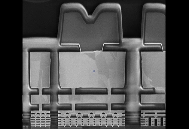
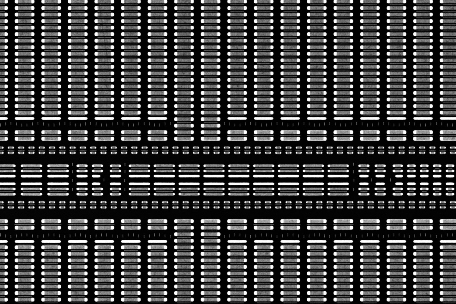
Based on our research activities, we carry out in-depth system-level and advanced component-level analysis. Using the state-of-the-art tools developed within our research projects, we assess individual components for reliability, originality, IP violations, and error analysis. Our security laboratory is certified according to Common Criteria – Evaluation Assurance Level 6 (CC-EAL6), enabling scientific investigation of security-relevant components concerning their trustworthiness. Through full-surface planar preparation of the IC's metal layers and subsequent chip scanning, we can conduct a GDSII conversion to check for IP violations and suspicion of malicious circuit manipulation.
IC analysis and package reliability testing

View of the Raith Velion FIB-SEM with the front cover open
Package & chip level analysis
Analyses at component level
- Failure and damage analysis using light-optical and X-ray inspection, metallographic microsection preparation and scanning electron microscope, as well as electrical measurement at IC level
- State-of-the-art tools for analyzing individual components with regard to reliability, originality and IP violation
- Security laboratory certified according to Common Criteria - Evaluation Assurance Level 6 (CC-EAL6) for the examination of security-relevant components
- Full-surface planar preparation of individual metal layers of an IC with GDSII conversion and examination for IP violation or malignant manipulation
- In-depth analysis of robustness and ESD investigations in cooperation with the electrical measurement technology expert group
Analysis at component level
- Electrical characterization of SMD components
- Originality testing of IC and packages
- IC technology analysis
- De-packaging
- De-processing of ICs: from the active side (de-layering) or rear side (chip thinning)
- Full-surface scanning electron microscopy imaging of entire metallization layers and their preparation
- Patent analysis
BSI Site Certification of Fraunhofer EMFT
Information on scope, results and status of the BSI Site Certification.
Entry with status, validity, and associated certificate documents - BSI Site Certification - Fraunhofer EMFT
BSI test and certification report on IT security of the site - BSI Site Certification Report - Fraunhofer EMFT
Scope and measures of the BSI site certification - BSI Site Security Target Lite - Fraunhofer EMFT


